Wire bonding is an electrical interconnect technology developed by microelectronics industry and today used excessively in ( solid state) detector construction. It allows to interconnect electronic chips, printed circuit boards, pitch adapters and solid state sensors (usually silicon).
A basic ingredient, common to most bonding methods is the transfer of ultrasonic energy via the resonating bond tool to the interface between the bond wire and the bond pad in order to form a metallurgical bond, a kind of micro weld.
An excellent introduction to the topic is provided by G. Harman: Wire bonding in Microelectronics, McGraw-Hill, 2nd edition (1996)
Overview of the different bonding methods
Generally one distinguishes between wedge and ball bonding technologies
.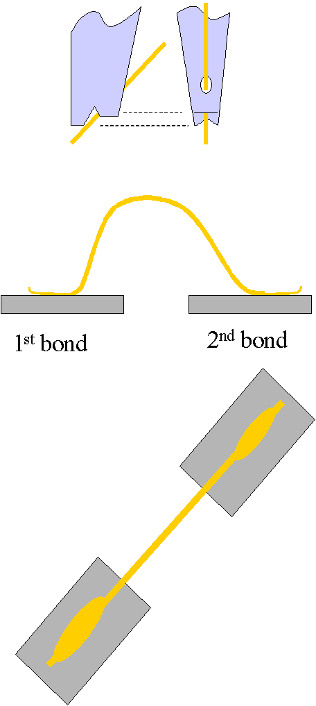 <-
wedge bonding
<-
wedge bonding 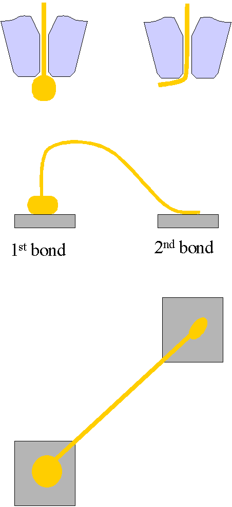 <-
gold ball
<-
gold ball
The bond tools (upper part of schematics) and the way the wire is held are very different. The orientation of the wedge tool (left schematic) defines the bond direction. The bond head of a wedge bonder must therefore be oriented in a straight line from the 1st to the 2nd bond, before the 1st bond can be made. This requires a more complex rotating bond head than for ball bonders (right schematic), where the wire can be bent and drawn from the first bond in any direction. The heavier mechanics and the more complex bond head movement slow down the wire bonding process. In ball bonding the first bond is made by means of a ball which is formed before be means of an electrical spark, while the second bond resembles a wedge bond.
Currently the DSF bondlab is performing exclusively Ultrasonic wedge bonding with Aluminum wires. For completeness we give a brief historical overview of the different bonding technologies.
Thermocompression (TC) bonding. Developed in 1957 for gold wire on gold gold pads, but practically not in use anymore. As there is no ultrasonic energy involved, it requires a combination of high temperature (>300°C) and high force at the bond interface.
Ultrasonic (US) wedge bonding has been used in microelectronics industry since about 1960, mainly for device production, but was there later replaced by thermosonic gold ball bonding (see below). In High Energy Physisics (HEP) applications, US wedge bonding is the predominant method, as it doesn't require any substrate heating and therefore is very versatile. US wedge bonding is mainly used to bond Al wires (diameter in the range 17 - 75 um and even over 0.5mm in special cases!) to Al or Au bond pads. This page shows a complete wedge bonding sequence (in a very schematic way).
Thermosonic (TS) gold ball bonding was introduced in 1970 and is today widely used in industry, mainly for packaging chips. Compared with TC, the ultrasonic activation allows to lower the interface temperature to 125-220°C.
Tape Automated Bonding (TAB) uses thin Cu beams instead of wires. The beams are held in place by thin polymer tapes (usually Polyimide) and form a microcable. Invented in the 1960s and existing in several variations, TAB has so far been limited to niche applications because of its relatively high cost and low flexibility (every change of the bond pattern layout requires new masks (and tapes). The STAR experiment (BNL) and ALICE are employing a form of TAB technology.
Flip chip bonding, often also referred to as bump bonding currently provides the highest connection density. Invented in the mid 1960s, the technology uses bumps (conductive polymers, Indium or solder bumps, microballs) instead of wired to bond the flipped chip to a substrate. In HEP the flip chip technology is so far exclusively used in the construction of Si pixel detectors, where a Si sensor, segmented as area array of individual diodes need to be connected to the readout chip, correspondingly segmented.