The basic concept
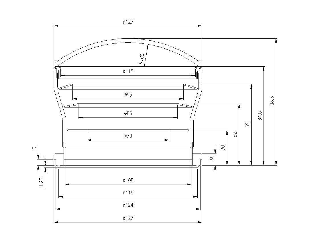
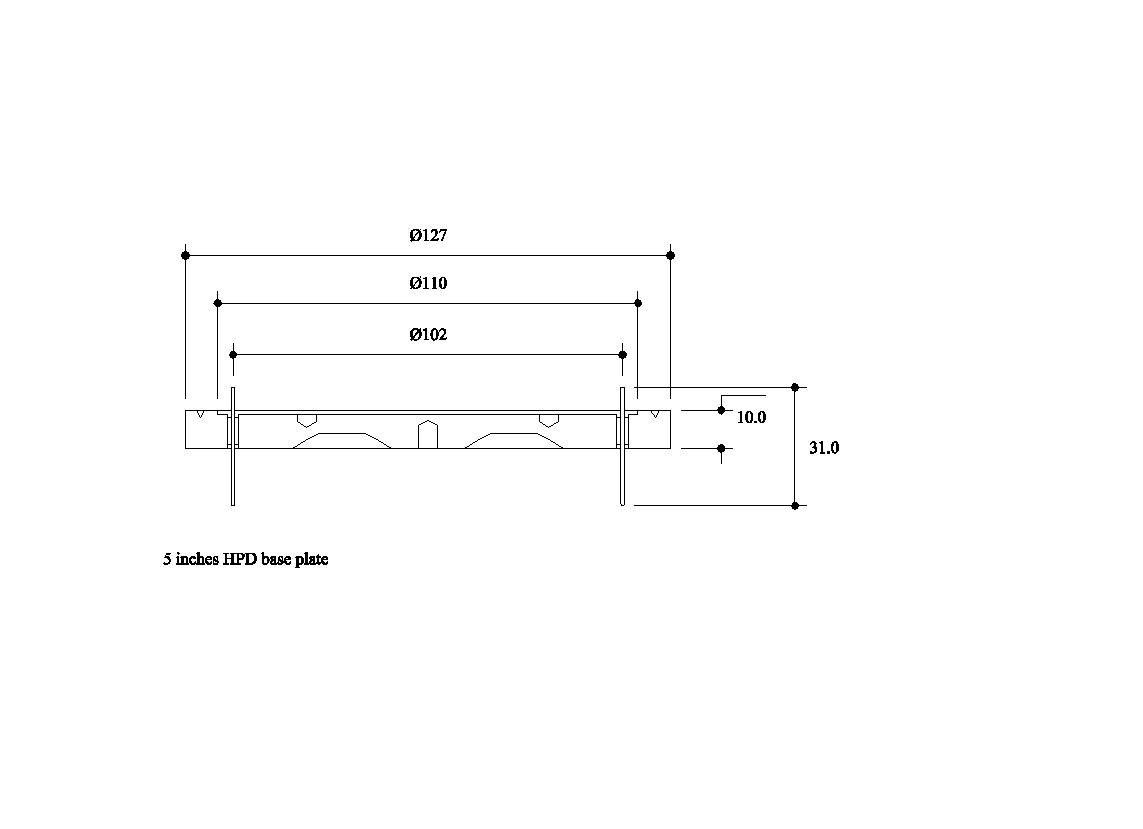
The Pad HPD is a fast, large area, highly pixelized Hybrid Photodiode. Photoelectrons emitted from the bialkali cathode are accelerated towards the silicon sensor by a fountain shaped electric field. The field configuration is such that a 2.3 fold demagnified image of the photocathode is produced on the silicon sensor.The fast low noise analogue electronics is integrated inside the vacuum envelope (see drawing). The multiplexed signals are readout through 40 vacuum feedthroughs on the baseplate (see drawing).
The HPD is fabricated by means of an external vacuum evaporation process. The baseplate is sealed to the envelope after photocathode processing applying a special cold indium sealing technique.
The basic design features
| overall diameter | 5" = 127 mm |
| active diameter | 114 mm |
| entrance window | borosilicate glass, cut off < 250 nm |
| field configuration | fountain shape, defined by 4 ring electrodes |
| demagnification | 2.3 |
| photocathode | bialkali (K2CsSb), semi-transparent |
| silicon sensor | 300 mm thick, 50 mm diam., 2048 pads, 1 x 1 mm |
| current electronics | 16 Viking VA3 chips, ENC <300 e |
| final electronics | 16 SCT128A chips, LHC specifications, ENC ~ 650 e |
| max. HV | ca. 20 kV |
| S/N ratio | ~ 15 at 20 kV, using VA3 chip |
Since September 2000 the Pad HPD is fabricated with a modified glass envelope (2nd generation). Equipped with a robust entrance window seal and a simplified electrode configuration (2 ring electrodes + 1 bleeder wire), it allowed to overcome leak proplems and high voltage limitations observed with the 1st generation envelopes.
A ceramic version of the 5-inch Pad HPD is also under development.
The readout electronics
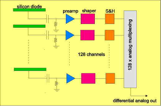
The Pad HPD is equipped with a low noise analogue readout chain. An analogue readout scheme has been chosen because it offers a number of advantages (pulse hight information, photon counting, flexible response to noise, also common mode noise, easy debugging, presice). These points are crucial if one deals with very small signals, as it is the case for a HPD.
Because the final LHC speed readout chip, the SCT128A, was not available when the project started, the relatively slow VA2 / VA3 chip (IDE AS) was used for the first tests. Meanwhile the SCT128A chip has become available. First tests indicate that it perfectly fits the Pad HPD requirements.
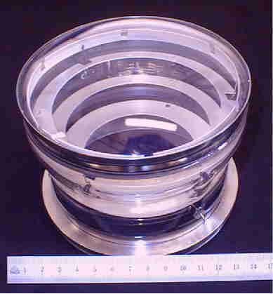
The vacuum envelope (1st generation)
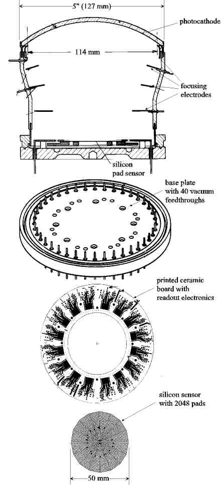
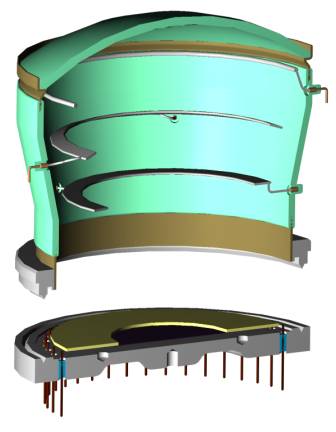
Exploded view of the Pad HPD
The vacuum envelope (2nd generation)
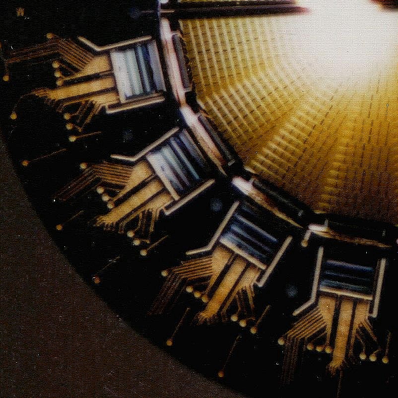
A quarter of the silicon sensor plus 4 readout chips
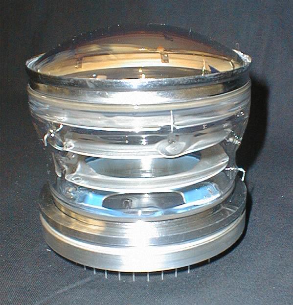
A sealed HPD with full readout electronics and bialkali photocathode